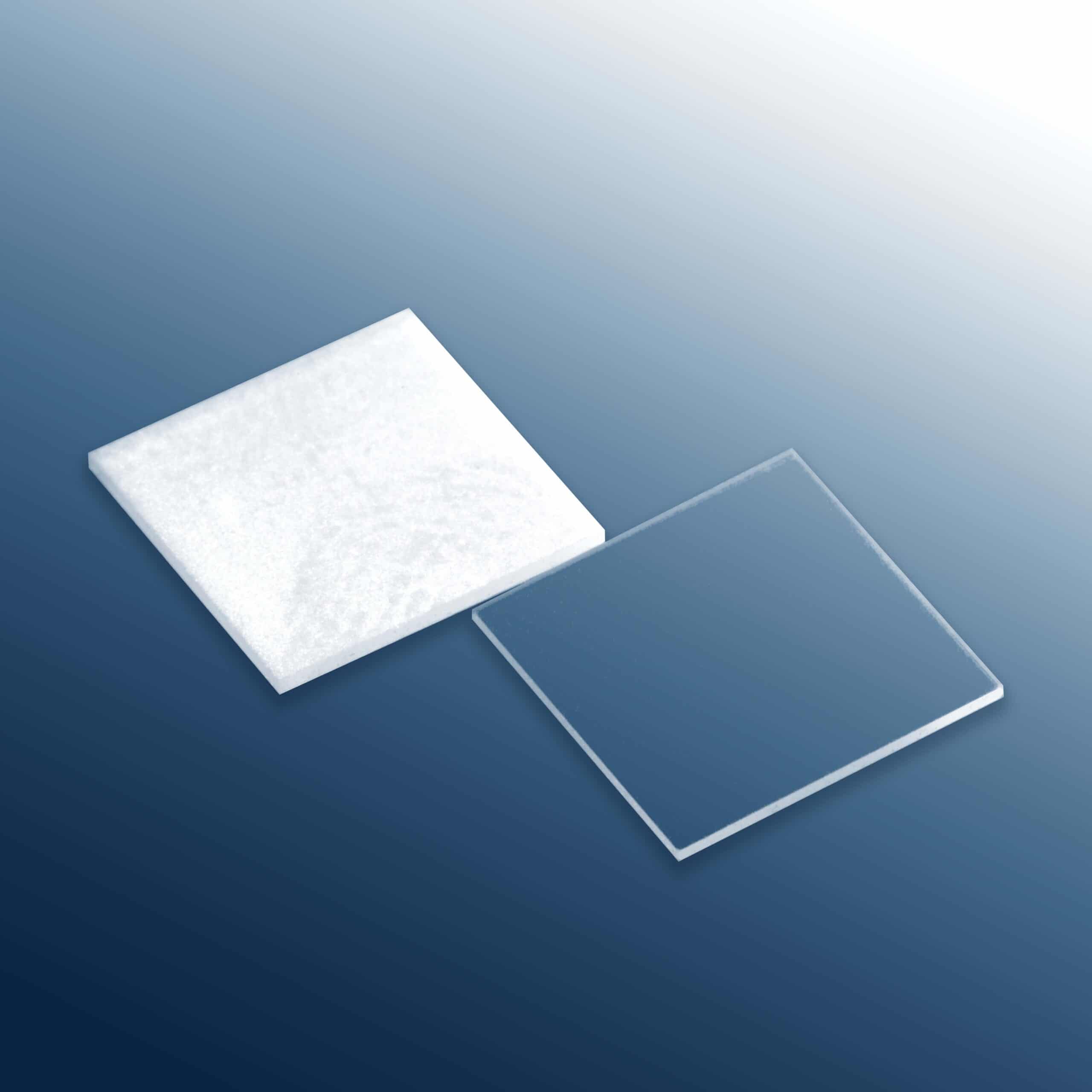
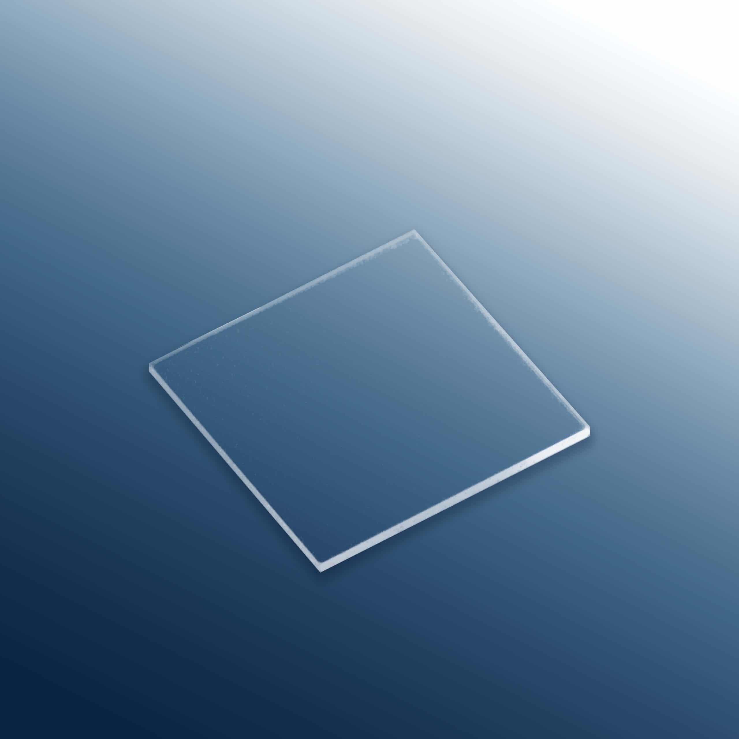
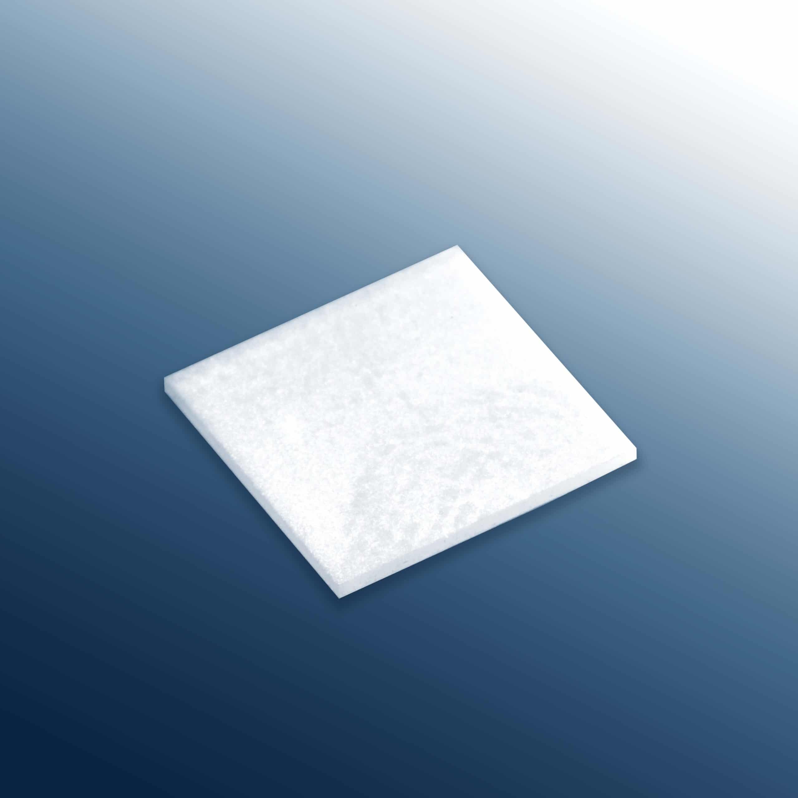
Sapphire’s mechanical strength, thermal stability, electrical insulation and lattice compatibility make it an ideal substrate for advanced semiconductor and optoelectronic devices, including LEDs, RF components, power electronics and high-frequency circuits.
With precise polishing and flatness, our sapphire substrates are used as a base material for thin-film depostion (e.g. GanN-on-Sapphire for LEDs, RF devices and microelectronics). Sapphire substrates are designed to support the growth of semiconducts layers and provide excellent thermal and electrical insulation.
We provide one-side polished (OSP) or double-side polished (DSP) sapphire substrates to meet specific epitaxial layer growth requirements.
We offer a wide range of standard sapphire substrates in stock.
Contact us to request quote for custom sapphire substrates tailored to your specifications.
- No minimum order quantity required.
- A $15.00 handling fee applies to orders totaling less than $100.00 before shipping.
Where Is the Best Place to Buy Sapphire Substrates?
Sourcing single crystal sapphire substrates requires more than finding a vendor with inventory. You need precise polishing, accurate crystal orientation, reliable dimensional tolerances, and a supplier who understands exactly how substrate specifications affect downstream processing. AdValue Technology supplies sapphire substrates for semiconductor, photonics, electronics, optical, and research applications where surface quality and dimensional consistency matter.
Why Single Crystal Sapphire Substrate Quality Matters So Much
Sapphire substrates serve as the foundation for some of the most technically demanding processes in modern manufacturing. GaN-on-Sapphire epitaxial growth for LED fabrication, RF component development, and high-frequency circuit design all depend entirely on substrate quality. Surface roughness, crystal orientation accuracy, and flatness aren't optional specifications. They directly control the quality of the epitaxial layers grown on top of the substrate. A poorly polished or misoriented substrate introduces defects that compound through every subsequent process step.
That's precisely why choosing an expert supplier matters as much as choosing the right material.
C Plane and A Plane. Both Done Right.
Crystal orientation is one of the most critical specifications in sapphire substrate selection. AdValue Technology offers substrates in both C Plane and A Plane orientations, covering the two most widely used configurations in semiconductor and photonics applications.
C-plane sapphire, also written as (0001), is widely used for GaN-based LED, laser diode, and nitride semiconductor epitaxy. A-plane sapphire is selected for applications requiring a different crystallographic orientation, anisotropic optical or mechanical behavior, or specific film-growth conditions. Because sapphire orientation can directly affect thin-film growth, optical behavior, and device performance, customers should confirm the required plane, miscut angle, surface finish, and polishing specification before ordering.
| Orientation |
Designation |
Key Characteristics |
Typical Applications |
| C-Plane |
(0001) |
Most widely used orientation for nitride semiconductor epitaxy |
GaN-based LEDs, laser diodes, nitride semiconductor devices |
| A-Plane |
(11-20) |
Different crystallographic orientation; anisotropic optical and mechanical behavior |
Specialized film-growth conditions, optical applications requiring specific orientation |
Having both orientations available from a single trusted supplier simplifies procurement and eliminates the inconsistency risk that comes with using multiple vendors.
One-Side Polished and Double-Side Polished Options
AdValue Technology gives you full control over surface finish with both One-Side Polished (OSP or 1SP) and Double-Side Polished (DSP or 2SP) configurations available across the lineup.
| Polish Configuration |
Abbreviation |
Description |
Best For |
| One-Side Polished |
OSP / 1SP |
Mirror-quality finish on the growth surface only |
Most epitaxial deposition applications where only one surface requires a polished finish |
| Double-Side Polished |
DSP / 2SP |
Mirror-quality finish applied to both faces |
Optical applications, transmission measurements, and processes requiring access to both faces |
AdValue Technology stocks both configurations so you order exactly what your process specifies.
Performance Properties That Drive Advanced Applications
Every single crystal sapphire substrate from AdValue Technology delivers the core properties that make sapphire the material of choice across high-performance industries:
- Exceptional mechanical strength that withstands the physical stresses of wafer handling, bonding, and processing without cracking or chipping
- Outstanding thermal stability that maintains substrate integrity through high-temperature epitaxial growth processes
- Excellent electrical insulation that isolates device layers and prevents signal interference in RF and high-frequency applications
- Suitability as a widely used substrate for GaN and other nitride semiconductor epitaxy, especially when surface finish, orientation, and process conditions are properly controlled
- Superior surface flatness that enables uniform thin-film deposition across the entire substrate area
These properties make AdValue's sapphire substrates a natural fit for LEDs, laser diodes, power electronics, RF components, high-frequency components, optical windows, and selected communication-related applications.
Custom Specifications for Non-Standard Applications
Standard catalog dimensions don't cover every application. AdValue Technology offers custom sapphire substrates for researchers and engineers whose process requirements fall outside the standard size range. Non-standard lengths, widths, thicknesses, and surface finish specifications are all available on request. Share your requirements with their team and they'll produce substrates matched precisely to your specifications.
That flexibility makes AdValue Technology a genuine development partner, not just a parts supplier.
No Minimum Order Quantity for Standard Sapphire Substrates
AdValue Technology maintains a wide range of standard sapphire substrates in stock, with no minimum order quantity required. This is especially helpful for researchers, engineers, and product-development teams that need small quantities for evaluation before moving to larger orders. A $15.00 handling fee applies to orders under $100.00 before shipping.
Reach the AdValue Technology Team
AdValue Technology is headquartered in Tucson, Arizona and serves customers across the U.S. and internationally. Their team brings specialized expertise in crystals, advanced ceramics, and high-performance substrates. Reach them directly at +1 (520) 514-1100 or at sales@advaluetech.com for orders, custom specifications, or technical guidance.
Browse the full single crystal sapphire substrate lineup at advaluetech.com and place your order today.

 Technical Info