No products in the cart.
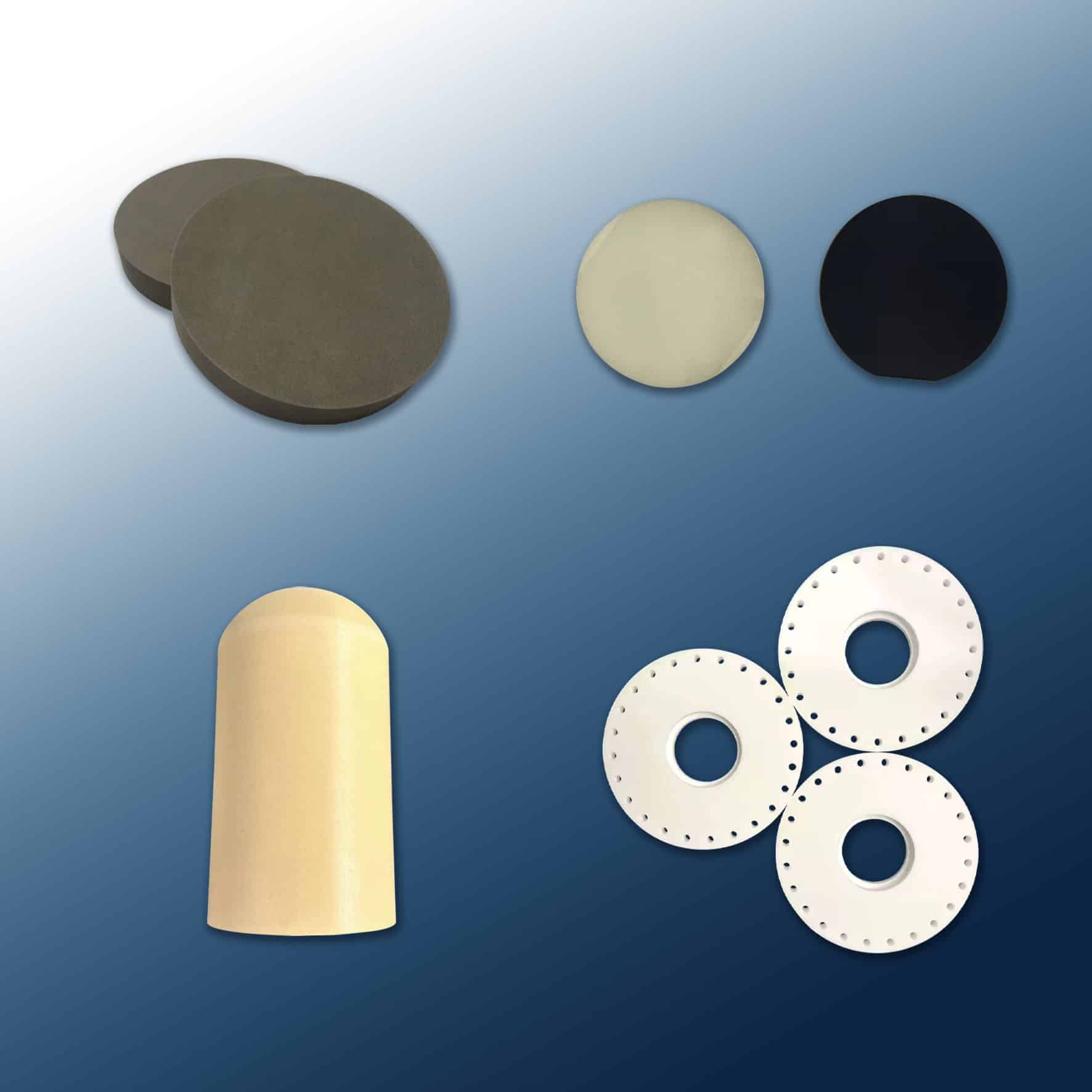
Beyond our primary product lines, we offer an expanded selection of materials to support a wide range of research and production needs. The following list represents commonly requested options. If you are looking for a material not included here, please contact us to discuss your requirements.
AdValue Technology can also provide materials below.
Dense Magnesium Oxide (MgO) ceramic is a highly durable, and thermally stable ceramic material composed primarily of magnesium oxide. Renowned for its high melting points, superior hardness, and strong resistance to chemical attack, MgO ceramic is ideal for a wide range of demanding industrial applications such as metallurgy, electronics, energy, and chemical processing. Common uses of MgO ceramics include high-temperature furnace components, crucibles, electrical insulation in heating elements, and protective coatings. Magnesium Oxide products offer outstanding thermal performance, withstanding temperatures up to 2200 °C (4000 °F).
AdValue Technology supplies high-purity Magnesium Oxide (MgO) products (>98% purity) in a variety of sizes and shapes. Please contact us to request a quote for custom MgO products.
At AdValue Technology, we offer high purity (>99.99%) single crystal (monocrystalline) Silicon Carbide (SiC) wafers. Compared to traditional silicon wafers, Silicon Carbide wafers deliver superior performance, excelling under higher temperatures, voltages, and frequencies, making them ideal for high-power and high-efficiency applications.
We supply 4H-SiC wafers in standard diameters of 2”, 3”, 4”, 6” and 8”. Custom specifications can be discussed upon request.
In addition to monocrystalline wafers, AdValue Technology also supplies polycrystalline silicon carbide products engineered for mechanical strength and thermal shock resistance. We provide both Sintered SiC (SSiC) and Reaction-Bonded SiC (RB-SiC) ceramics:
Featuring ~99% SiC, dense microstructure, exceptionally high mechanical strength, superior thermal conductivity, and excellent chemical resistance. SSiC is ideal for applications such as high-end kiln furniture, mechanical seals, pump components and space parts.
A composite of SiC and free silicon (Si), RB-SiC offers good strength and good chemical resistance, though lower than sintered SiC. Its thermal conductivity is also lower. Reaction-Bonded SiC serves as a cost-effective alternative for large kiln furniture (setter plates, beams, saggers, etc.) and cost-sensitive components.
AdValue Technology delivers high-quality silicon carbide products in a range of sizes and shapes. Please contact us to discuss your application requirements or request a quote for custom SiC products.
Silicon Nitride is an advanced technical ceramics known for handling extreme environments where metals or polymers would fail. The material exhibits a few unique advantages:
AdValue Technology supplies custom Silicon Nitride products, available in a wide range of dimensions and shapes. Our Silicon Nitride offerings include bearings, turbine components, industrial nozzles and valves, cutting tools, automotive components, etc. Please contact us to request a quote for custom Silicon Nitride products.
Zirconia Toughened Alumina (ZTA) is an advanced ceramic composite that combines the high hardness and wear resistance of alumina (Al₂O₃) with the excellent fracture toughness of zirconia (ZrO₂). By incorporating a controlled amount of zirconia into the alumina matrix, ZTA significantly improves mechanical properties such as strength, toughness, and resistance to crack propagation compared to pure alumina ceramics.
ZTA is widely used in demanding applications where traditional ceramics would fail under mechanical stress, such as in cutting tools, wear-resistant components, and armor systems. It offers an ideal balance between hardness, toughness, and chemical stability, making it a material of choice for both industrial and medical applications.
AdValue Technology supplies custom zirconia toughened alumina (ZTA) products in a wide range of dimensions and shapes. Please contact us to request a quote for custom ZTA products.
Titanium Boride (TiB₂) is a highly valued ceramic material known for its exceptional combination of hardness, high melting point, excellent thermal conductivity, and chemical stability. TiB₂ products are typically characterized by extreme hardness, outstanding wear and erosion resistance, and the ability to withstand high temperatures without significant degradation. Additionally, TiB₂ possesses excellent electrical conductivity for a ceramic material, enabling its use in specialized applications like cathodes for aluminum smelting and electrodes in electrochemical processes.
Titanium boride products are often used as wear-resistant components, armor materials, electrodes for aluminum smelting, aerospace and electronic components, and crucibles and containers for molten metals.
AdValue Technology can provide custom Titanium Boride products in a wide range of dimensions and shapes. Please contact us to request a quote for custom Titanium Boride products.
Sintered Yttrium Oxide (Y2O3) products are high-performance ceramic materials distinguished by their excellent heat resistance, exceptional thermal stability, great chemical inertness, low thermal expansion and superior optical properties. With a melting point exceeding 2400 ℃, Yttrium Oxide remains chemically stable even when exposed to highly active metals (such as Ti, Al, Hf, Nb, etc.) at elevated temperatures. Additionally, Yttrium Oxide exhibits high transparency in the infrared spectrum and strong resistance to laser-induced damage.
Due to these unique characteristics, sintered Yttrium Oxide products are widely used as crucibles and linings for high-temperature metal processing, components for crystal growth systems, parts for plasma processing equipment, and laser host materials and optical windows.
AdValue Technology can provide custom Yttrium Oxide products in a wide range of dimensions and shapes. Please contact us to request a quote for custom Yttrium Oxide (Y2O3) products.
AdValue Technology offers high-performance thin film-deposited ceramic substrates that combine the inherent durability of ceramics with the versatile functionality of thin films. These substrates are essential components in a wide array of advanced technologies, including microelectronics, optoelectronics, and sensor systems.
Utilizing ion sputtering and ion-assisted evaporation techniques, metal films (such as Cr/Ni/Au and Ti/Pt/Au) are deposited onto various ceramic materials, including Alumina (Al₂O₃), Aluminum Nitride (AlN), Zirconia (ZrO₂), Beryllium Oxide (BeO), Ferrite, and microwave substrates. Our capabilities include the fabrication of fine-line circuits, precise metallization, ceramic edge-side graphics, sidewall coatings, and double-sided graphical circuits.
For custom ceramic film products designed to meet your specific requirements, please contact us to request a quote.
MgO | SiC | Si₃N₄ | ZTA | TiB₂ | Y₂O₃ | Thin Film-Deposited Ceramic Substrates
AdValue Technology goes well beyond standard ceramics. In addition to our core lineup of alumina, fused quartz, boron nitride, and sapphire, we supply a comprehensive range of advanced specialty materials including:
Metals and polymers each have their limits. Metals conduct electricity, expand significantly with temperature, and can corrode or oxidize in harsh environments. At the same time, polymers soften and degrade at moderate temperatures.
Advanced ceramics occupy a performance space neither material class can match. They combine high-temperature stability, electrical insulation, hardness, chemical inertness, and in some cases unique properties like infrared transparency or electrical conductivity. These properties are what make advanced ceramics a viable solution for applications in semiconductor processing, power electronics, aerospace, medical devices, and high-temperature manufacturing.
Yes, we can. Custom component design and manufacturing is a core capability at AdValue Technology. For every material in this lineup, custom shapes, sizes, and specifications are available.
Whether you need a one-off prototype for a research project or a production-volume order for a manufacturing process, our team can work with you on a tailored solution. Reach out with your design requirements, drawings, or performance targets and we will take it from there.
Magnesium Oxide, commonly known as magnesia, is a dense refractory ceramic prized for its very high melting point, excellent thermal stability, and strong performance in demanding thermal environments. It belongs to a class of oxide ceramics capable of maintaining its structural integrity and performance under extreme heat and aggressive chemical conditions. MgO is used across metallurgy, electronics, energy systems, and chemical processing wherever conventional materials fall short at high temperatures.
AdValue Technology supplies MgO ceramic products at greater than 98% purity. That high-purity standard ensures minimal contamination risk in sensitive applications such as electrical insulation in heating elements, high-temperature crucibles, and protective coatings where material integrity directly affects performance outcomes.
MgO ceramic products from AdValue Technology are rated for use up to 2,200°C (4,000°F). That extreme temperature capability places MgO among one of the most thermally capable oxide ceramics available.
Very few materials maintain structural integrity and electrical insulation at those temperatures, which is why MgO is a trusted choice for demanding furnace environments, high-temperature crucibles, and refractory applications.
AdValue Technology MgO ceramic products deliver a strong set of high-temperature performance characteristics:
MgO ceramic components serve a wide range of high-temperature and high-purity applications:
AdValue Technology supplies Silicon Carbide in three distinct forms, each serving a different set of applications:
Monocrystalline SiC wafers are single-crystal substrates grown with a highly ordered crystal structure used for wide-bandgap semiconductor devices. AdValue Technology carries 4H-SiC wafers, the most commercially significant polytype, in standard diameters of 2 inches, 3 inches, 4 inches, 6 inches, and 8 inches, with custom specifications available.
These wafers are the foundation of next-generation power electronics devices including electric vehicle inverters, solar inverters, industrial motor drives, and 5G infrastructure equipment. SiC outperforms traditional silicon in power applications by handling higher voltages, higher temperatures, and higher switching frequencies with significantly lower energy loss.
4H-SiC is the dominant commercial SiC polytype for power electronics because it combines a wide bandgap of approximately 3.26 eV, high critical electric field, strong thermal conductivity, favorable carrier mobility, and mature large-diameter wafer availability.
These properties translate directly into power devices that switch faster, run hotter, and waste less energy as heat compared to silicon-based equivalents. The 4H crystal structure also allows more reproducible and controllable doping during device fabrication, which is critical for manufacturing high-performance, reliable power semiconductors.
| Property | Sintered SiC (SSiC) | Reaction-Bonded SiC (RB-SiC) |
|---|---|---|
| SiC Content | Approximately 99% | SiC plus free silicon (Si) |
| Mechanical Strength | Exceptionally high | Good, lower than SSiC |
| Thermal Conductivity | Superior | Good, lower than SSiC |
| Chemical Resistance | Excellent | Good, lower than SSiC |
| Typical Applications | Mechanical seals, pump components, space parts, high-end kiln furniture | Large kiln furniture, setter plates, beams, saggers, cost-sensitive components |
| Cost | Higher | More cost-effective |
SiC products from AdValue Technology serve a broad range of industries requiring extreme performance:
Silicon Nitride is one of the most mechanically capable structural ceramics available. It combines high strength, outstanding toughness, excellent thermal shock resistance, wear resistance, and good thermal conductivity in a lightweight package that weighs significantly less than most metals performing similar structural roles.
Engineers and designers reach for Si₃N₄ when they need a material that maintains its structural integrity at high temperatures, survives rapid thermal cycling, and resists wear over long service lives. It is a genuinely versatile engineering ceramic that works where metals and polymers simply cannot.
Silicon Nitride delivers a compelling combination of structural and thermal properties:
Si₃N₄ thrives in applications where structural performance, weight savings, and thermal resilience all matter at the same time:
Alumina is a workhorse ceramic with excellent hardness and chemical resistance, but it is relatively brittle and susceptible to thermal shock and mechanical impact. On the other hand, Silicon Nitride offers better fracture toughness, higher thermal shock resistance, and greater strength at elevated temperatures.
In applications such as bearings, turbine components, and cutting tools where mechanical stress and thermal cycling are both present, Si₃N₄ consistently outperforms alumina. When the cost of component failure is high, Si₃N₄ justifies the investment.
Zirconia Toughened Alumina is a composite ceramic material that incorporates a controlled amount of zirconia (ZrO₂) into an alumina (Al₂O₃) matrix. That combination is a deliberate engineering choice. Alumina contributes excellent hardness, wear resistance, and chemical stability.
Zirconia contributes fracture toughness through a transformation toughening mechanism that stops cracks from propagating through the material. The result is a ceramic that delivers the best of both worlds: hard like alumina, but far more resistant to cracking and impact than pure alumina alone.
Zirconia undergoes a phase transformation from tetragonal to monoclinic crystal structure when stress is applied. In ZTA, zirconia particles are retained in their metastable tetragonal phase within the alumina matrix.
When a crack begins to propagate through the material and reaches a zirconia particle, the stress at the crack tip triggers the transformation. That transformation expands the zirconia particle slightly, which compresses the crack tip and resists further crack growth. This transformation toughening mechanism gives ZTA its characteristic resistance to catastrophic brittle failure, setting it clearly apart from pure alumina ceramics.
ZTA delivers a balanced set of mechanical and chemical properties:
ZTA excels in applications where both hardness and resistance to impact or crack propagation are required:
Titanium Diboride is a transition metal boride ceramic that occupies a unique position in the advanced materials world. It is one of the hardest ceramics commercially available, with hardness values typically between 25 and 35 GPa, while also being electrically conductive, which is highly unusual for a ceramic material. Its combination of exceptional hardness, high melting point exceeding 3,000°C, excellent thermal conductivity, and outstanding wear and erosion resistance makes TiB₂ a highly specialized material for applications where extreme conditions are the norm.
TiB₂ stands out in the ceramics world for its exceptional combination of properties:
Unlike oxide ceramics such as alumina or zirconia, TiB₂ has a metallic bonding character in addition to its covalent ceramic bonds. The partially filled d-orbital electrons in titanium contribute to electrical conductivity in a way that oxide ceramics cannot replicate.
This gives TiB₂ electrical resistivity values in the range of 10 to 15 microohm centimeters, which is comparable to some metallic conductors. That conductivity allows TiB₂ to function in electrode, cathode, electrical-contact, and electrochemical applications where most ceramics would simply be insulators.
TiB₂ serves in specialized applications that leverage its unique combination of hardness, conductivity, and thermal stability:
Yttrium Oxide, also known as yttria, is a rare earth oxide ceramic with a melting point exceeding 2,400°C and a remarkable combination of optical, thermal, electrical, and chemical properties. Depending on processing, Y₂O₃ can be produced as dense ceramic components, plasma-resistant coatings, or transparent ceramics for selected infrared and laser applications. This combination makes yttria valuable in crystal growth, reactive metal processing, semiconductor plasma equipment, high-temperature systems, and advanced optical or laser applications.
Y₂O₃ delivers a distinctive suite of properties that few other ceramics can match:
Crystal growth for advanced electronic and optical materials requires crucibles and liners that remain chemically stable at very high temperatures without contaminating the melt. Y₂O₃ is chemically stable when in contact with highly reactive metals like titanium, aluminum, hafnium, and niobium at elevated temperatures, making it one of the very few ceramic materials that can serve as a crucible or liner when growing crystals of these reactive materials.
Y₂O₃ is used both as a host material for laser-active rare earth ions and as a damage-resistant optical component in high-power laser systems. When doped with neodymium (Nd) or ytterbium (Yb), Y₂O₃ ceramics function as gain media in solid-state lasers.
As an undoped material, when processed into high-density transparent ceramics, its strong resistance to laser-induced damage and high infrared transparency make it valuable for optical windows, lenses, and protective elements in high-power laser setups.
Y₂O₃ finds use across several high-performance industries where its unique combination of properties is required:
Thin film-deposited ceramic substrates are high-performance ceramic base materials that have been precisely metallized using physical vapor deposition (PVD) techniques. Metal films are deposited onto the ceramic surface at the nanometer to micrometer scale, creating electrically conductive traces, pads, and circuit patterns with exceptional dimensional precision.
These substrates combine the thermal, mechanical, and electrical benefits of advanced ceramics with the conductivity and solderability of metal films, making them the substrate of choice for demanding microelectronics, optoelectronics, and sensor applications.
AdValue Technology produces thin film-deposited ceramic substrates using two established physical vapor deposition methods:
AdValue Technology offers two proven metal film layer systems designed for strong adhesion, reliable solderability, and excellent electrical performance:
Both systems are industry-standard metallization stacks used in high-reliability microelectronic packaging, optoelectronic device, RF, and sensor assemblies.
AdValue Technology can apply thin film metallization to a broad range of ceramic substrates to suit different application requirements:
| Substrate Material | Key Advantage for Thin Film Applications |
|---|---|
| Alumina (Al₂O₃) | Cost-effective, widely used substrate with excellent mechanical stability and dielectric properties |
| Aluminum Nitride (AlN) | High thermal conductivity for power electronics and LED applications requiring efficient heat dissipation |
| Zirconia (ZrO₂) | Tough, strong substrate for applications requiring mechanical robustness |
| Beryllium Oxide (BeO) | Exceptional thermal conductivity for specialized high-performance thermal management substrates; requires appropriate handling controls |
| Ferrite | Magnetic substrate for microwave and RF filter applications |
| Low-Loss Microwave Ceramics | Low-loss dielectric substrates optimized for high-frequency microwave circuit applications |
AdValue Technology’s thin film deposition capabilities go well beyond simple flat surface metallization. Our process supports a range of sophisticated circuit and pattern configurations:
These substrates serve as the foundation for some of the most advanced miniaturized electronic systems being built today:
Yes. Custom thin film ceramic substrate products are available to meet specific customer requirements. Whether you need a non-standard substrate material, a unique circuit pattern, a specific metallization stack, or a custom substrate size, AdValue Technology can develop a solution tailored to your application. Get in touch with our technical team and send us your specifications so we can communicate all available options with their corresponding lead times.
AdValue Technology maintains an extensive inventory of standard products across our specialty materials portfolio. Standard in-stock items typically ship within 1 to 2 business days. For custom components, specialty grades, or materials requiring specific processing, lead times vary and are communicated promptly upon inquiry.
Yes. AdValue Technology ships both within the United States and internationally. Whether your lab, fab, or manufacturing facility is located domestically or abroad, our logistics capabilities are set up to deliver specialty ceramic and materials products to you wherever they are needed, with expedited shipping options available.
AdValue Technology is a full-service specialty materials supplier. Our broader product catalog includes: