Sapphire’s mechanical strength, thermal stability, electrical insulation and lattice compatibility make it an ideal substrate for advanced semiconductor and optoelectronic devices, including LEDs, RF components, power electronics and high-frequency circuits.
With precise polishing and flatness, our sapphire substrates are used as a base material for thin-film depostion (e.g. GanN-on-Sapphire for LEDs, RF devices and microelectronics). Sapphire substrates are designed to support the growth of semiconducts layers and provide excellent thermal and electrical insulation.
We provide one-side polished (OSP) or double-side polished (DSP) sapphire substrates to meet specific epitaxial layer growth requirements.
We offer a wide range of standard sapphire wafers in stock.
Contact us to request quote for custom sapphire wafers tailored to your specifications.
- No minimum order quantity required.
- A $15.00 handling fee applies to orders totaling less than $100.00 before shipping.
Where Is the Best Place to Buy Sapphire Wafers?
Not every sapphire wafer supplier can meet the standards that advanced technology applications actually demand. Surface finish, crystal orientation accuracy, total thickness variation, and substrate purity are not secondary considerations. They are the variables that determine whether your downstream process works reliably or introduces defects, yield losses, or performance inconsistencies. For researchers, engineers, and manufacturers who need single crystal sapphire wafers they can depend on, AdValue Technology offers a supply source built around precision, traceability, and material quality.
A Material That Demands a Precise Supply Chain
Single crystal sapphire is grown through highly controlled processes that determine the final crystallographic structure, optical clarity, and surface quality of every wafer. A supplier that cuts corners on crystal growth conditions, wafer slicing tolerances, or surface polishing introduces variability that compounds through every stage of device fabrication. AdValue Technology sources and supplies single crystal sapphire wafers with the dimensional and crystallographic control that precision applications require, whether the end use is LED epitaxy, power semiconductor fabrication, optical windows, or specialized research substrates.
What Sets AdValue Technology Apart as a Sapphire Wafer Supplier
Several factors distinguish AdValue Technology from generic catalog suppliers when it comes to single crystal sapphire wafers.
-
Orientation options that match your process requirements:
AdValue Technology offers sapphire wafers in the orientations that matter most to industry, including C-plane (0001), A-plane (1120), R-plane (1102), and M-plane (1010). Each orientation has specific epitaxial, optical, and structural advantages. Having access to multiple orientations from a single supplier simplifies procurement and keeps specification traceability consistent across projects.
-
Surface quality built for demanding downstream processes:
Wafer surface roughness directly affects epitaxial layer quality, optical performance, and device reliability. AdValue Technology supplies single crystal sapphire wafers with epi-ready polished surfaces and controlled surface roughness specifications, reducing the need for additional processing steps before use.
-
Dimensional control that protects process consistency:
Total thickness variation, bow, warp, and edge profile are not afterthoughts in AdValue Technology specifications. Tight dimensional tolerances reduce wafer-to-wafer variability in deposition, lithography, and bonding steps, which translates directly into more predictable yields and fewer process interruptions.
-
Custom specifications for non-standard requirements:
Standard catalog dimensions serve a wide range of customers, but many applications require something more specific. AdValue Technology works with customers to accommodate custom diameters, thicknesses, orientations, and surface finishes when standard offerings do not match the process requirement. That flexibility makes AdValue Technology a practical long-term partner rather than a one-time catalog vendor.
-
Flexible order quantities for research and development:
Development programs and academic research often need small quantities of high-quality substrates without committing to production volumes. AdValue Technology accommodates orders at the scale your project actually requires, from small research quantities through production-level supply.
Physical Properties That Make Sapphire Indispensable
Understanding why sapphire wafers are so widely specified across demanding applications starts with the material itself. Single crystal sapphire (Al2O3) combines a set of properties that few other substrate materials can match:
-
Melting point of approximately 2040 degrees Celsius:
Supporting use in high-temperature deposition and processing environments where other substrates fail.
-
Mohs hardness of 9:
Making sapphire highly resistant to surface scratching during handling, processing, and end-use environments.
-
Excellent optical transmission from ultraviolet through near-infrared wavelengths:
Enabling use in optical windows, sensors, and optoelectronic device substrates.
-
High thermal conductivity compared to glass and many other optical materials:
Supporting applications in power electronics and high-brightness LED substrates where heat management matters.
-
Strong chemical resistance to most acids and alkalis under standard processing conditions:
Which simplifies wet cleaning and etching steps during device fabrication.
-
Electrical insulation characteristics:
Making sapphire a preferred substrate for gallium nitride and other wide-bandgap semiconductor devices.
Applications Across the Industries That Rely on Sapphire Wafers
AdValue Technology single crystal sapphire wafers serve a wide range of technically demanding applications:
-
LED and solid-state lighting:
C-plane sapphire is the dominant substrate for gallium nitride LED epitaxy. Consistent surface quality and orientation accuracy directly affect luminous efficiency and wafer-level yield in high-volume LED production.
-
Power semiconductor devices:
Wide-bandgap semiconductors grown on sapphire substrates are used in power electronics requiring high breakdown voltage, high switching speed, and operation at elevated temperatures.
-
Optical windows and domes:
Sapphire optical windows provide broadband transmission combined with extreme mechanical durability, making them the specified material for aerospace sensors, laser systems, and high-pressure optical access ports.
-
RF and microwave devices:
Sapphire substrates support the fabrication of microwave integrated circuits and resonators where low dielectric loss, dimensional stability, and crystallographic uniformity are required.
-
Research and development substrates:
Laboratories working on novel thin film materials, 2D materials, and emerging semiconductor technologies use sapphire wafers as a well-characterized, chemically stable platform for deposition and characterization experiments.
-
Medical and industrial sensors:
Sapphire components appear in pressure sensors, flow sensors, and harsh-environment optical probes where the combination of chemical resistance, hardness, and optical transmission makes alternative materials inadequate.
Consistency Across Orders, Not Just Within a Single Shipment
Lot-to-lot consistency is an important but sometimes overlooked consideration when evaluating a sapphire wafer supplier. A single high-quality shipment provides limited value if subsequent orders vary in surface roughness, crystal orientation, dimensions, or other critical specifications. AdValue Technology maintains quality control processes designed to deliver consistent material across orders, giving process engineers a reliable foundation for process qualification and production scaling.
For applications where substrate quality must remain consistent and predictable, AdValue Technology provides single crystal sapphire wafers with the precision, traceability, and supplier responsiveness that modern fabrication environments require. From small research batches to production supply, AdValue Technology is the source worth specifying.
Reach AdValue Technology at +1 (520) 514-1100 or at sales@advaluetech.com to place an order, request a custom specification, or discuss your application requirements.
Browse the full single crystal sapphire wafer lineup at advaluetech.com and order today.
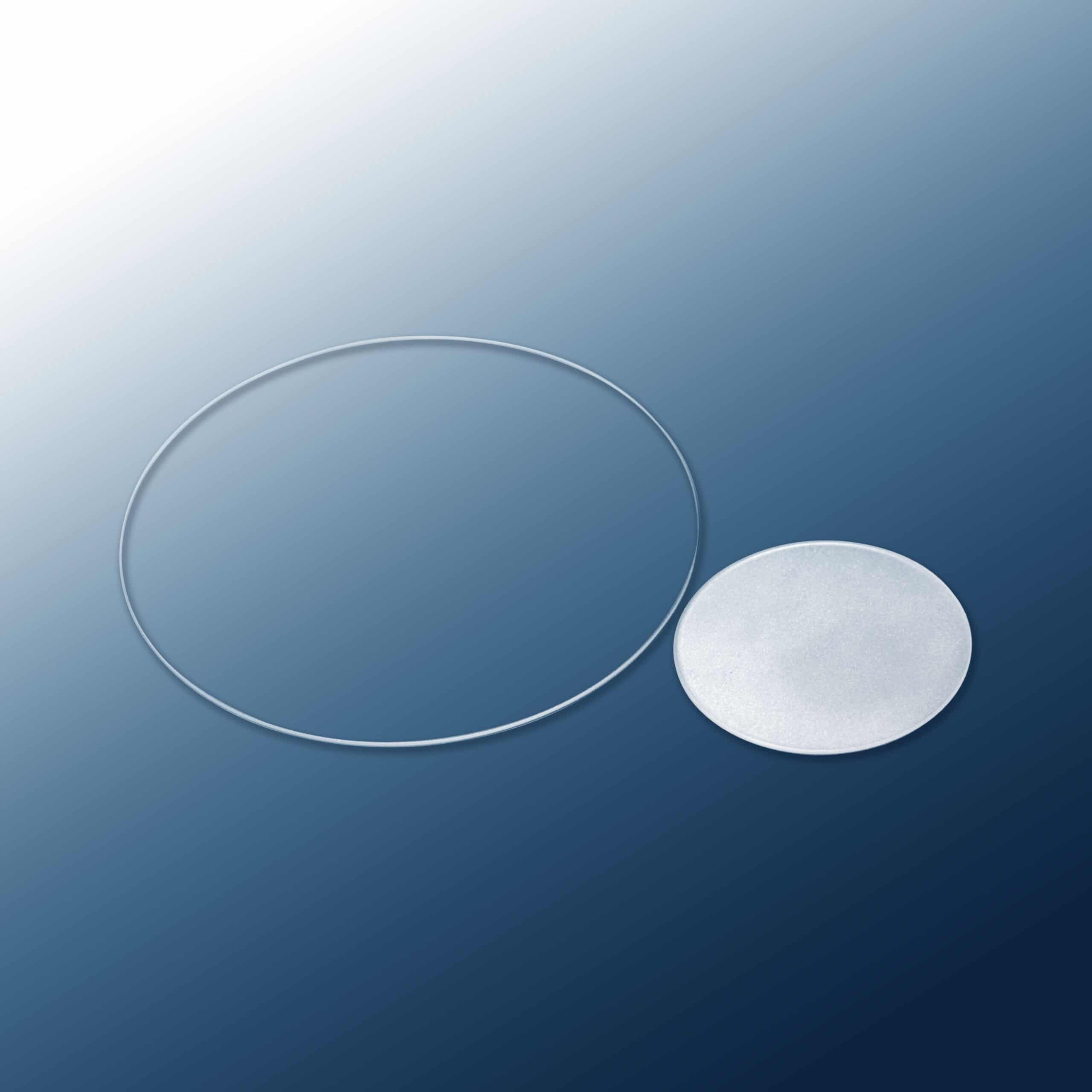
 Sapphire Wafers Double Sides Polished (2SP)
 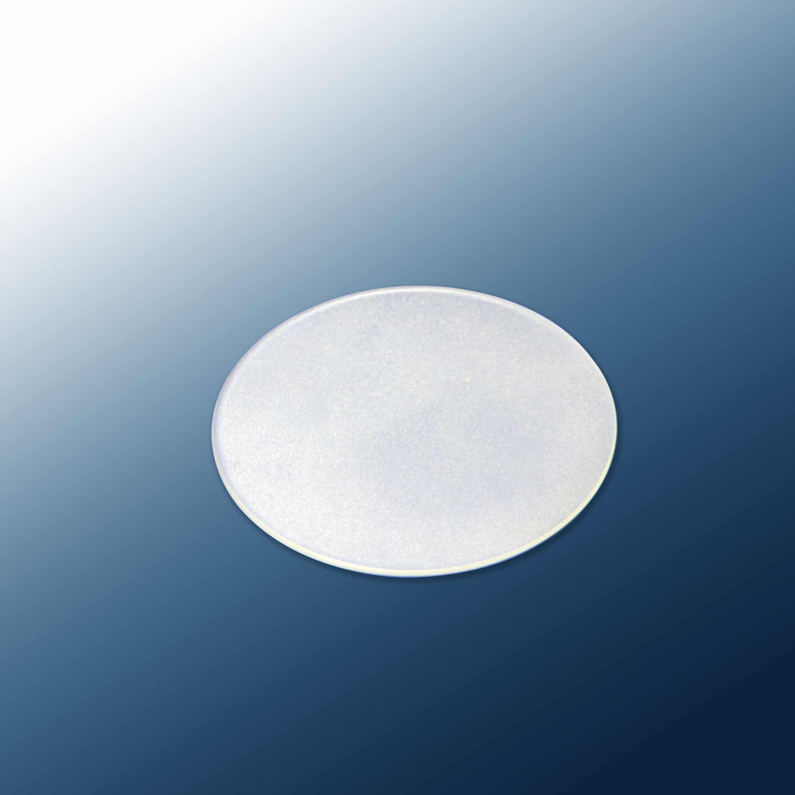 Sapphire Wafers Single Side Polished (1SP)



 Technical Info