You’ve walked under LED streetlights, used a smartphone with an impossibly scratch-resistant camera lens, and watched displays that render color with striking clarity. What you probably haven’t considered is the thin, polished disc of single-crystal material making it all possible. In millions of electronic devices and virtually every blue and white LED produced today, that material is a sapphire wafer.
Thank you for reading this post, don't forget to subscribe!The global sapphire wafer market hit $1.62 billion in 2025 and is on track to reach nearly $3 billion by 2033, growing at a 7.92% compound annual rate. That growth isn’t hype. It’s the direct result of physics that competing materials simply haven’t been able to match.
A sapphire wafer is a thin, precision-polished disc of synthetic corundum, chemically expressed as α-Al₂O₃ (aluminum oxide), produced in single-crystal form for use as a substrate in semiconductor and optoelectronic device fabrication. It shares its chemical formula with ordinary alumina ceramic but differs in one critical way: its atomic structure is continuous, uninterrupted, and highly ordered throughout the entire crystal.
That single-crystal structure is what makes sapphire wafers so valuable. Polycrystalline materials contain grain boundaries, defects, and inconsistencies that introduce noise, scatter light, and reduce device reliability. Single-crystal sapphire eliminates grain boundaries and greatly improves uniformity . Every atom sits in its intended position within the hexagonal lattice, delivering consistent, predictable behavior from wafer center to edge. For semiconductor epitaxy, that uniformity isn’t a preference. It’s a requirement.
Sapphire’s hexagonal crystal system also means its properties change with orientation. That anisotropy lets engineers select the specific crystal cut that matches their device architecture, unlocking performance advantages not available in isotropic materials.
Sapphire wafers don’t exist in nature at the purity and scale electronics manufacturing requires. Three primary crystal growth methods dominate commercial production:
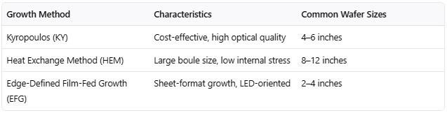
After growing the raw crystal boule, manufacturers slice it using precision diamond wire saws, followed by lapping, grinding, edge shaping, and polishing. For epitaxial applications, the wafer surface is typically finished by chemical mechanical polishing, or CMP, to achieve an ultra-smooth, low-defect surface. Typical specifications may include front-side surface roughness below 1 nm RMS, total thickness variation, or TTV, within tight micrometer-level limits, and controlled bow, warp, and crystal orientation.
Sapphire scores 9 on the Mohs hardness scale, making it the hardest oxide crystal and second in hardness only to diamond. In wafer fabrication environments, that hardness means sapphire resists micro-scratching during cassette handling, robotic transfer, and equipment contact. Fewer surface defects mean less particle contamination in cleanroom environments and better epitaxial layer quality.
Compressive strength reaches 2000 MPa. Thinner wafers can be processed without the breakage risk that limits other brittle substrate materials, improving yield efficiency in high-volume production lines.
Sapphire transmits light from approximately 150 nm (deep UV) through the visible spectrum and into the mid-infrared at ~5500 nm. That broad transparency window makes it uniquely suited to optoelectronic applications where the substrate must transmit emitted light rather than absorb it. Silicon is opaque to visible wavelengths. Glass cuts off in the UV range. Sapphire transmits both, without mechanical compromise.
Sapphire’s electrical resistivity exceeds 10¹¹ Ω·cm at room temperature. It’s a near-perfect insulator. That property is the foundation of silicon-on-sapphire technology, eliminating the substrate leakage currents and parasitic coupling that constrain RF performance in standard silicon CMOS devices.
Thermal conductivity sits at approximately 42 W/m·K at room temperature, depending on crystal orientation. This is sufficient for effective heat dissipation in standard LED and RF applications. With a melting point above 2000°C and excellent chemical and thermal stability, sapphire can survive the high-temperature MOCVD processes used for GaN epitaxial growth without degrading or outgassing into the device layer.
The c-plane orientation (0001) is the dominant substrate face for LED manufacturing. It presents a surface with approximately 14-16% lattice mismatch with gallium nitride. That mismatch is manageable through buffer layer engineering and patterned surface technology. C-plane sapphire supports consistent, high-quality GaN epitaxial growth under standard MOCVD conditions, which is why it became the global standard for commercial LED production.
Standard c-plane wafer diameters run at 2″, 3″, 4″, and 6″. The 4″ format leads current LED fab production. Larger formats up to 12″ are available from HEM-grown boules for research and defense applications.
A-plane (11-20) sapphire is used in certain GaN epitaxy applications to support the growth of nonpolar or semipolar GaN orientations. These device structures can reduce polarization-induced electric fields that are commonly associated with conventional C-plane GaN, improving performance in selected LED, laser diode, and high-electron-mobility device architectures. R-plane (1-102) sapphire supports silicon epitaxial growth with lattice parameters suited to silicon-on-sapphire (SOS) fabrication.
Orientation selection is an engineering decision with direct device performance consequences. Choosing correctly from the start avoids costly rework later in the fabrication process.
Blue and white LED technology made possible by breakthroughs in gallium nitride-based semiconductor materials, with sapphire serving as the practical substrate that enabled high-volume GaN epitaxial growth. The researchers who developed efficient blue LEDs using this approach received the 2014 Nobel Prize in Physics, recognizing a breakthrough that transformed global lighting from energy-hungry incandescent sources to efficient solid-state systems.
Sapphire provides the stable, chemically inert foundation on which GaN epitaxial layers grow. Its thermal stability withstands MOCVD deposition temperatures exceeding 1000°C without degrading. Its electrical insulation enables lateral current flow device structures. Its optical transparency allows a portion of emitted photons to pass through the substrate rather than being absorbed by it.
GaN-on-sapphire remains one of the dominant technologies for commercial LED production because it delivers this combination of performance and cost-efficiency at scale. Bulk GaN substrates offer better lattice match but cost exponentially more per wafer. For high-volume LED manufacturing, sapphire wins.
Flat sapphire substrates work. Patterned sapphire substrates (PSS) work significantly better for GaN-based LED manufacturing . PSS involves etching microscale surface patterns, typically cone, pyramid, or volcano shapes, into the sapphire surface before GaN epitaxial growth begins. Those patterns deliver two measurable performance improvements simultaneously.
First, they redirect threading dislocations away from the active device region. PSS helps reduce threading dislocation density in the GaN epilayer. The patterned surface promotes lateral epitaxial overgrowth and can bend or terminate some dislocations, reducing the number of defects that propagate into the active device region. Research published in Nanoscale via RSC Publishing documents threading dislocation density (TDD) reductions ranging from 30% to over 92% depending on the PSS geometry used.
Second, the patterned interface scatters and redirects internally reflected light outward, dramatically improving light extraction efficiency. Documented performance improvements include:
These aren’t incremental gains. They’re manufacturing-scale improvements that directly affect how competitive a product is in the global LED market.
Silicon-on-sapphire (SOS) technology uses a thin epitaxial silicon layer grown on an insulating sapphire substrate, creating a fully insulating base for CMOS circuit fabrication. Because sapphire provides excellent electrical isolation, SOS devices can reducethe substrate leakage, parasitic capacitance, or noise coupling that limit performance in standard bulk silicon processes. These advantages are especially valuable in RF, microwave, mixed-signal, and radiation-tolerant electronics.
According to Microwave Journal’s analysis of SOS RF technology, SOS-based designs achieve prsk DC-to-DC converter efficiency exceeding 92% at 800 KHz, RF switch on-resistance below 100 mΩ at 1A, and the ability to integrate RF switching with power management circuitry on a single die. These advantages make SOS the substrate technology of choice for satellite communication systems, military radar electronics, and high-performance mobile device RF front-end modules.
Sapphire’s hardness makes it the go-to material for scratch-resistant surfaces in premium consumer devices. Smartphone camera lens covers, fingerprint sensor windows, and luxury watch crystals all use sapphire components for the same reason: almost nothing scratches them during normal use. As wearable electronics become more sophisticated and consumers expect longer device lifespans, sapphire’s role in consumer electronics will only expand.
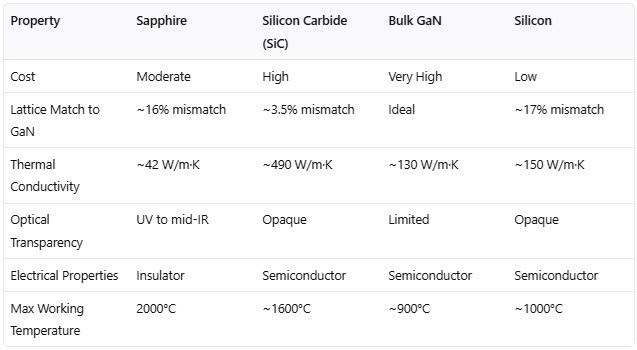
SiC offers better lattice match to GaN and superior thermal conductivity but is opaque and significantly more expensive. Bulk GaN is ideal for GaN devices but difficult to produce at scale. Silicon is cheap but completely unsuitable for light-emitting applications. Sapphire occupies the optimal position for the majority of LED and RF semiconductor applications where cost, optical transparency, and thermal performance must align.
The numbers tell a clear story. The global sapphire wafer market was valued at $1.62 billion in 2025 and is projected to reach $2.98 billion by 2033, driven by a 7.92% CAGR. Asia Pacific holds the largest regional share at 36.5%, fueled by large-scale LED production in China, Taiwan, and South Korea. North America follows at 26.4%, led by defense, aerospace, and RF semiconductor demand.
Growth drivers shaping the market include:
Sapphire wafers serve as substrates for GaN-based LED manufacturing, silicon-on-sapphire RF electronics, laser diodes, optical sensors, and precision consumer electronics components. Their combination of optical transparency, electrical insulation, mechanical hardness, and thermal stability makes them uniquely suited for applications where other substrates fail to meet combined performance requirements.
Sapphire is optically transparent across the wavelengths that LEDs emit, thermally stable during MOCVD deposition, chemically inert in process environments, and available at a cost that makes high-volume production economically viable. Silicon is opaque. Bulk GaN is expensive. SiC costs more and doesn’t transmit visible light. Sapphire hits the performance-cost balance that large-scale LED production demands.
A patterned sapphire substrate is a wafer with microscale patterns etched into its surface before GaN epitaxial growth. These patterns reduce threading dislocation density in the GaN film by redirecting crystal defects, and they improve light extraction efficiency by scattering internally reflected photons outward. PSS technology can deliver over 200% improvement in light extraction compared to flat substrates.
C-plane (0001) sapphire is the industry standard for LED applications. It supports consistent GaN growth under standard MOCVD conditions and comes in the wafer sizes LED fab equipment is designed around. A-plane wafers are used for nonpolar or semipolar GaN structures. R-plane wafers support silicon-on-sapphire CMOS fabrication.
Standard sizes are 2″, 3″, 4″, and 6″ diameter. Four-inch is the most common in active LED production lines. Wafer thickness typically ranges from 430 to 650 µm depending on diameter. Larger formats up to 12″ are available for research, defense, and high-power applications using HEM-grown boules.
In SOS technology, a thin silicon film is grown on a fully insulating sapphire base. That insulating foundation reduces substrate leakage currents and noise coupling that limit RF performance in bulk silicon devices. As a result, SOS circuits achieve higher isolation, lower power consumption, and better signal integrity for high-frequency applications.
Yes. Sapphire’s melting point temperature is over 2000°C, far exceeding the 1000°C to 1100°C MOCVD deposition temperatures used for GaN growth. Its thermal conductivity of ~42 W/m·K provides adequate heat dissipation for standard LED applications. It also resists the reactive gas environments used in MOCVD chambers without outgassing or surface degradation.
Your epitaxial layers are only as good as the substrate beneath them. Inconsistent surface flatness, hidden defects, or substandard purity create yield problems that compound throughout your fabrication process. Getting the substrate right at the start is the most cost-effective decision in any LED or semiconductor production workflow.
AdValue Technology supplies high-purity sapphire components and specialty materials engineered for advanced research and production environments. Whether you need precision sapphire substrates for LED epitaxy, custom-cut wafer geometries, or laser-machined sapphire components with tight dimensional tolerances, their materials expertise and in-house laser machining capabilities cover your full range of application requirements. Standard materials ship within 1 to 2 business days with expedited options available for time-sensitive projects.Don’t let substrate quality become the bottleneck in your production. Contact AdValue Technology today to discuss your sapphire wafer specifications and find materials engineered for your exact application.