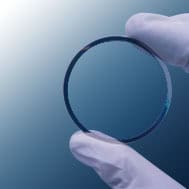
At AdValue Technology, we offer high quality diamond substrates which excel in the most demanding applications – from precision tools to cutting-edge electronics.
With a unique combination of mechanical strength, thermal properties, and electrical performance, our diamond substrates are engineered to meet the rigorous standards of today’s most advanced industries.
Key Features of Diamond Substrates
Extreme Hardness – Hardest material known, providing unmatched wear resistance
Highest Thermal Conductivity of any material – Over 10 x higher than copper, ensuring superior heat dissipation
High Electrical Insulation – Ideal for high-voltage and high-frequency applications
Wide Bandgap (~5.5 eV) – Significantly higher than silicon or gallium nitride
High Breakdown Voltage – Suitable for high-power, high-temperature devices
Strong Chemical Inertness – Resistant to most acids, bases, and solvents
High Radiation Resistance – Maintains performance in extreme environments
The unmatched properties make diamond substrates ideal for high-performance electronics, thermal management systems, optical applications, and radiation detection.
Material Performance Comparison
Thermal Conductivity W/(m∙K)
Moh’s Hardness
Thermal Expansion Coefficient (106/K)
Silicon Carbide
490
9.5
4.5
Cu
400
3
18
Diamond
1800-2000
10
1
Available Diamond Substrates
1. Diamond Substrates for Heat Spreaders
Diamond’s exceptional thermal conductivity and extremely low thermal expansion make it the ideal material for advanced heat spreader applications.
Type
Single Crystal (HPHT/CVD)
Thermal conductivity
>2000 W/m K
Size Available
0.15*0.15~25*25 mm
Thickness
0.1~1.0 mm
Tolerance
+/-0.05 mm
Face Orientation
(100)/(111)
Off Angle
<1°
Roughness
Ra<1 nm
Coefficient of Thermal Expansion at 25°C
1.0*10-6/°C
Type
Polycrystalline
Thermal conductivity
>1500W/m K
Size Available
0~75 mm
Thickness
0.2~2.0 mm
Tolerance
+/-0.05 mm
Roughness
Ra<10 nm
Coefficient of Thermal Expansion at 25°C
1.0*10-6/°C
Thermal conductivity
>700W/m K
Size Available
0~57 mm
Thickness
0~5.0 mm
Tolerance
+/-0.05 mm
Roughness
Ra<50 nm
Coefficient of Thermal Expansion at 25°C
2.0~2.2.0*10-6/°C
Conductivity
Conductive
2. Diamond Substrates for Windows
Diamond windows offer superior heat dissipation and greater bandwidth compared to traditional materials like sapphire and Boron Nitride. They enable longer part life, lower energy loss and lighter designs.
Type
Single Crystal/Polycrystalline
Size Available
0~25 mm/75 mm
Thickness
0.1~2.0 mm
Spectral Transparency
>70% (225 nm to Far IR)
Refractive Index
2.38 (IR range)
Dielectric Constant
5.7
Loss Tangent
<5*10-5
Roughness
Ra<10 nm
Thermal Conductivity
>2000/>1500 W/(m·K)
Type
220 GHz, 340 GHz, 660 GHz, 850 GHz, etc.
Size Available
Dia 0.5 mm~25 mm
S Parameter
S21 ≥-1.5 dB, S11 ≤-15 dB @220 GHz
Bandwidth
≥20 GHz @220 GHz
Vacuum Degree
<1*10-10 Pa/m3-s
Dielectric Constant
5.7
Loss Tangent
<5*10-5
Thermal Conductivity
>2000 W/(m·K)
3. Diamond Products for Semiconductor
Diamond single crystals are ideal for semiconductor, detector, and quantum sensing technologies due to diamond’s many unique advantages, including wide bandgap, high electron saturation velocity, large carrier mobility, low dielectric constant, and exceptional radiation resistance.
Type
HPHT
CVD
Size
0.15*0.15~25*25 mm (100) 0.15*0.15~15*15 mm (111)
0.15~0.15 ~ 22*22 mm
Thickness
0.06~1.0 mm
0.06~1.0 mm
Off Angle
(100)/(111) +/-1°
(100)/(111) +/-1°
Roughness
<1 nm
<1 nm
FWHM
<50 arcsec
<120 arcsec
TTV
<30 µm
<30 µm
WARP
<10 µm
<10 µm
Enhance your next-generation devices with the power of diamond technology.
Contact us today to discuss your application and request a quote.
Frequently Asked Questions About Diamond Substrates
What are diamond substrates, and what makes them unique compared to other substrate materials?
Diamond substrates are engineered diamond materials used as a foundational platform for advanced electronic, optical, and thermal applications. They serve as a base on which devices, coatings, or components are built, especially in environments where conventional substrates cannot meet the thermal, electrical, or environmental demands.
What makes diamond substrates unique compared to other materials is their unmatched combination of physical, thermal, electrical, and chemical properties. Diamond is the hardest known material, providing exceptional wear resistance and durability. It also has the **highest thermal conductivity of any material—more than ten times higher than copper—**which allows it to dissipate heat extremely efficiently, a critical advantage in high-power, high frequency and high-temperature devices.
In addition, diamond substrates offer excellent electrical insulation, a wide bandgap (~5.5 eV), and a high breakdown voltage, making them ideal for high-voltage and high-frequency electronics. Their low thermal expansion ensures dimensional stability under thermal stress, while broad optical transparency from UV to IR, chemical inertness, and radiation resistance enable reliable performance in extreme environments.
Together, these properties make diamond substrates a premium solution for cutting-edge electronics, thermal management, optics, and radiation detection, outperforming traditional materials such as silicon, sapphire, or ceramic substrates.
Which industries commonly use diamond substrates from AdValue Technology?
Diamond substrates are used across several high-performance and advanced technology industries that demand exceptional thermal, electrical, and mechanical properties. Industries that commonly use diamond substrates from AdValue Technology include:
Semiconductor and Electronics Manufacturing – for high-power, high-frequency, and high-temperature devices where superior heat dissipation and electrical insulation are critical.
Power Electronics – including RF, microwave, and high-voltage systems that benefit from diamond’s wide bandgap and high breakdown voltage.
Aerospace and Defense – for electronics, sensors, and components that must perform reliably in extreme thermal, radiation, and environmental conditions.
Optics and Photonics – for UV to IR optical components requiring durability, transparency, and thermal stability.
Thermal Management Systems – as heat spreaders and substrates for applications with intense heat loads.
Radiation Detection and Nuclear Technologies – due to diamond’s high radiation resistance and long-term stability.
Precision Tools and Industrial Applications – where extreme hardness and wear resistance are essential.
These industries rely on diamond substrates to achieve higher performance, longer lifespans, and greater reliability than is possible with conventional substrate materials.
What key properties make diamond substrates ideal for demanding applications? Diamond substrates are ideal for demanding applications due to their extreme hardness, unmatched thermal conductivity, and high electrical insulation. They feature a wide bandgap (~5.5 eV), high breakdown voltage, and very low thermal expansion, which enhances reliability in high-power and high-temperature devices. Additionally, diamond offers wide optical transparency from UV to IR, strong chemical inertness, and excellent radiation resistance, making it suitable for the most advanced and extreme operating environments.
How does diamond’s extreme hardness benefit precision tools and electronics?
Diamond’s extreme hardness provides several key benefits in precision tools and electronics:
Cutting and Grinding Efficiency: Because diamond is the hardest natural material, it can cut, grind, or drill extremely hard substances like ceramics, carbides, glass, and stone with minimal wear. This allows precision tools (e.g., diamond-tipped drill bits, saws blades, or grinding wheels) to maintain sharpness and dimensional accuracy over long periods, improving both efficiency and consistency.
Extended Tool Life: Hardness directly reduces abrasion and wear, meaning diamond-coated or solid-diamond tools last much longer than conventional materials. This is critical in industries requiring high precision, such as aerospace, medical device manufacturing, and semiconductor fabrication, where tool degradation directly impacts quality and cost.
High-Precision Machining: Diamond tools can achieve ultra-smooth surfaces and fine tolerances because they deform very little under stress. This is crucial in electronics, optics, and micromechanical components, where even minor surface irregularities can affect performance.
Thermal Management in Electronics: Diamonds also have excellent thermal conductivity. In electronics, diamond can be used as a heat spreader or substrate to dissipate heat efficiently from high-power semiconductors, helping prevent overheating and improving device reliability.
Miniaturization and Microfabrication: Diamond’s mechanical stability and resistance to wear enable the fabrication and long-term stability of microscopic features in microelectronics, MEMS, and precision optical components, particularly in harsh or high-power operating environments.
In short, diamond’s combination of extreme hardness and thermal properties allows tools and electronics to operate with unmatched precision, durability, and performance.
Why is diamond’s thermal conductivity critical for high-power and high-temperature devices?
Diamond’s exceptionally high thermal conductivity—among the highest of any known material—is critical for high-power and high-temperature devices for several reasons:
Efficient Heat Dissipation: High-power electronics, such as power transistors, LEDs, and laser diodes, generate a lot of heat in a small area. Diamond’s thermal conductivity allows this heat to be quickly transferred away from sensitive components, preventing hotspots that can degrade performance or cause failure.
Maintaining Performance: Excessive heat can reduce the efficiency of semiconductors and other high-power devices. By conducting heat away rapidly, diamond helps maintain stable electrical characteristics, ensuring the device performs reliably even under heavy load.
Enabling Miniaturization: As electronic devices shrink, power density increases, making thermal management more challenging. Diamond’s ability to spread heat efficiently allows engineers to design smaller, more powerful components without overheating.
High-Temperature Operation: Some devices, like RF amplifiers, high-power LEDs, or certain sensors, operate at elevated temperatures. Diamond can tolerate and conduct heat away effectively at these temperatures, extending the device’s operational lifespan.
Reducing Cooling Requirements: By conducting heat efficiently, diamond can reduce the need for bulky heat sinks or active cooling systems, enabling more compact and energy-efficient designs.
In short, diamond’s thermal conductivity keeps high-power and high-temperature devices cool, stable, and reliable, which is essential for modern electronics, aerospace systems, and high-performance industrial applications.
How does diamond compare to copper and other materials for heat dissipation?
Diamond is exceptionally superior to most materials in terms of thermal conductivity, which makes it a standout choice for heat dissipation in high-power applications. Here’s a comparison:
Material
Thermal Conductivity (W/m·K)
Key Notes
Diamond
1000–2200
Highest known among bulk materials. Excellent for spreading heat quickly from hotspots in electronics.
Copper
~400
Very good conductor, commonly used in heat sinks, but still 2–5× less efficient than diamond.
Aluminum
~205
Lighter than copper, but about 5–10× less thermally conductive than diamond.
Silicon Carbide
~120–270
Used in high-power electronics; much lower than diamond but better than many ceramics.
Silicon
~150
Standard semiconductor; decent conductor but far below diamond.
Key Advantages of Diamond over Copper and Others:
Faster Heat Removal: Diamond can move heat away 2–5× faster than copper, which is crucial for preventing localized hotspots in microelectronics.
High-Temperature Stability: Unlike metals that can expand or degrade at very high temperatures, diamond maintains high thermal conductivity and structure integrity over a wide range of device operating temperature range.
Miniaturization Potential: By spreading heat more effectively, diamond enables higher power densities and smaller device footprints before thermal limits are reached, compared to conventional metal or ceramic heat spreaders.
In short, while copper is already excellent, diamond takes heat dissipation to the next level, combining ultra-high conductivity with stability under extreme conditions.
What electrical insulation advantages do diamond substrates offer?
Diamond substrates offer exceptional electrical insulation advantages, making them highly valuable in electronics, especially high-power and high-frequency applications. Here’s why:
Extremely High Electrical Resistivity: Diamond is an excellent electrical insulator, with resistivity typically exceeding 1012 Ω⋅cm10^{12}\ \Omega\cdot\text{cm}1012 Ω⋅cm. This prevents unwanted current leakage between components, which is critical for device reliability and safety.
High Breakdown Voltage: Diamond can withstand very high electric fields before breaking down, allowing it to insulate components in high-voltage or high-power circuits. This is especially important in power electronics and RF devices.
Low Dielectric Loss: Diamond has very low dielectric loss, meaning it doesn’t dissipate significant energy as heat when subjected to alternating electric fields. This property is crucial for high-frequency devices, such as microwave or RF circuits, where energy loss must be minimized.
Thermal-Electrical Synergy: Unlike many insulating materials that degrade under heat, diamond combines excellent insulation with outstanding thermal conductivity. This allows diamond substrates to both electrically isolate and efficiently remove heat from high-power components simultaneously—a rare combination.
Chemical and Mechanical Stability: Diamond is chemically inert and mechanically robust. It maintains its insulating properties even in harsh environments, including elevated temperatures, high fields, corrosive atmospheres, or high mechanical stress.
In summary, diamond substrates provide reliable electrical isolation while simultaneously handling extreme heat, making them ideal for advanced electronics like power transistors, high-frequency devices, and microelectronics where both insulation and thermal management are critical.
How does the wide bandgap of diamond benefit electronic and semiconductor applications?
Diamond’s wide bandgap (~5.5 eV) offers several important benefits for electronic and semiconductor applications:
High Breakdown Voltage: A wide bandgap means diamond can withstand very high electric fields before electrical breakdown occurs. This allows devices incorporating diamond to operate at much higher voltages than silicon (1.1 eV) or gallium arsenide (1.4 eV), which is critical for power electronics and high-voltage applications.
High-Temperature Operation: Wide bandgap materials can operate at much higher temperatures because they are less prone to thermal excitation of electrons across the bandgap. Diamond-based devices can function reliably in extreme thermal environments where silicon would fail.
Low Leakage Current: Diamond’s large bandgap reduces the number of thermally generated charge carriers, which lowers leakage currents in electronic components. This improves efficiency and reliability in both low- and high-power circuits.
High-Frequency Performance: Reduced parasitic conduction and low leakage help diamond-based transistors and RF devices to operate at higher frequencies with minimal signal loss.
Radiation Hardness: The wide bandgap, combined with diamond’s strong covalent bonding and high atomic displacement energy, makes diamond intrinsically more resistant to radiation damage, making it suitable for space, nuclear, and harsh industrial environments.
Energy-Efficient Devices: Because less energy is lost to heat through leakage and intrinsic carrier generation, diamond semiconductors can achieve higher efficiency, particularly in power conversion and high-performance electronics.
In short, diamond’s wide bandgap allows for high-voltage, high-temperature, high-frequency, and radiation-tolerant devices, combining performance advantages that few other materials can match.
Why is high breakdown voltage important for diamond-based devices?
High breakdown voltage is crucial for diamond-enabled devices because it determines how much electrical stress a material can withstand before it starts conducting uncontrollably, potentially leading to failure. Here’s why it matters:
Safe Operation at High Voltages: Devices like power transistors, diodes, and RF amplifiers often operate under high voltage. Diamond’s high breakdown voltage allows these devices to handle much higher voltages than silicon or other conventional semiconductors without risk of dielectric breakdown.
Reduced Risk of Device Failure: Electrical breakdown can cause permanent damage to circuits. Diamond’s ability to resist breakdown ensures reliability and longevity in high-power applications.
Compact, High-Power Designs: Materials with low breakdown voltage require larger devices or additional insulation to handle the same voltage. Diamond’s high breakdown voltage allows engineers to design smaller, more efficient devices while still safely managing high voltages.
High-Power Density Applications: In power electronics, energy must be managed in confined spaces. Diamond’s ability to sustain high voltage without failure enables high-power density circuits in areas like electric vehicles, aerospace, and industrial power systems.
Synergy with Thermal Conductivity: High-voltage devices generate heat. Diamond not only withstands high voltages but also efficiently conducts heat, allowing devices to operate safely under both electrical and thermal stress.
In essence, diamond’s high breakdown voltage allows electronic components to be smaller, more powerful, and more reliable, which is critical for cutting-edge high-power and high-frequency applications.
How does diamond’s low thermal expansion improve dimensional stability?
Diamond’s low thermal expansion—meaning it changes very little in size when heated or cooled—offers significant benefits for dimensional stability in precision devices:
Maintains Tight Tolerances: In high-precision tools, optics, and electronics, even tiny dimensional changes can affect performance. Diamond’s minimal expansion ensures components retain their exact shape and alignment across wide temperature ranges.
Reduces Mechanical Stress: Materials that expand or contract significantly can induce stress at interfaces or joints, potentially causing warping, cracking, or delamination. Diamond’s low thermal expansion minimizes these stresses, improving durability and reliability.
Stable Optical Performance: In optical systems, thermal expansion can shift lenses or mirrors, affecting focus or beam alignment. Diamond’s stability ensures consistent optical performance even under temperature fluctuations.
High-Temperature Applications: In electronics and power devices, localized heating is common. Diamond’s low thermal expansion prevents thermal distortion, which is critical for high-power, high-frequency, and high-temperature circuits.
Compatibility with Other Materials: Diamond’s low expansion makes it easier to combine with other materials that have similar or moderate thermal expansion coefficients, reducing the risk of failure in composite structures or bonded layers.
In summary, diamond’s low thermal expansion ensures precision, reliability, and long-term dimensional stability, which is essential in precision machining, optics, and high-performance electronics.
What optical applications benefit from diamond’s UV to IR transmission range?
Diamond’s wide optical transmission range—from ultraviolet (UV) through visible to infrared (IR) makes it ideal for a variety of optical applications where clarity, durability, and broad-spectrum performance are critical. Key applications include:
High-Power Laser Optics: Diamond’s transparency from UV to IR allows it to be used as windows, heat spreaders, and protective optics in high-power laser systems, including industrial cutting lasers, medical lasers, and scientific lasers, without significant absorption or damage.
UV Photonics and Inspection: I Diamond’s transparency into the deep UV and its chemical and radiation resistance make it suitable for UV optical windows, sensors, and photonics systems used in semiconductor inspection, metrology, and specialized lithography support optics.
Infrared (IR) Sensors and Windows: Diamond transmits effectively in the near and parts of the mid-IR range, making it ideal for thermal imaging systems, IR spectroscopy, and IR lasers. Its durability allows use in harsh environments where conventional IR optics might degrade.
High-Precision Optics: Diamond’s combination of optical clarity, low thermal expansion, and hardness enables precision windows and optical components that maintain alignment and performance under extreme conditions.
Harsh Environment Optics: Diamond can withstand high temperatures, abrasive conditions, radiation, and corrosive chemicals while remaining transparent across the UV–mid-IR spectrum, making it perfect for space instruments, industrial sensors, and defense optics.
Spectroscopy and Analytical Instruments: Broad spectral transmission allows diamond windows and prisms to be used in instruments that analyze light from UV through IR, enabling accurate measurements across multiple wavelengths.
In short, diamond’s broad UV–IR transmission, combined with its hardness and thermal stability, makes it a premium material for high-performance, durable optical applications across industries.
How does diamond’s chemical inertness improve performance in harsh environments?
Diamond’s chemical inertness—its resistance to corrosion, oxidation, and chemical attack—greatly enhances performance in harsh environments. Here’s how:
Resistance to Corrosion and Chemical Attack: Diamond does not react easily with most acids, bases, or solvents. This ensures that optical windows, sensors, and electronic substrates maintain their integrity and performance even in chemically aggressive environments.
Durability in Extreme Conditions: In industrial, aerospace, or marine applications, components may encounter heat, moisture, or reactive chemicals. Diamond’s chemical stability allows it to withstand these extremes without corrosion, swelling, or chemical degradation.
Maintains Optical Clarity and Surface Quality: For optical applications, exposure to harsh chemicals can cloud or damage traditional glass, polymers, or coatings. Diamond retains its UV–IR transparency, surface smoothness, and functional properties even under prolonged exposure to corrosive or reactive chemicals.
Longer Device Lifespan: Chemical inertness reduces wear and degradation over time, meaning diamond-based tools, electronics, and optics require less maintenance and have longer service life.
Compatibility with Aggressive Processes: Diamond components can tolerate many cleaning chemicals, etchants, and fabrication environments used in semiconductor processing and high-power photonics, except where diamond is intentionally etched using specialized plasmas or ion processes.
Safe for Extreme Thermal and Electrical Stress: Because diamond doesn’t react chemically under elevated temperature or electrical stress, it can operate reliably in high-power electronics, high-temperature sensors, and harsh industrial machinery.
In short, diamond’s chemical inertness ensures durability, stability, and consistent performance, even in environments that would degrade other materials quickly.
Why are diamond substrates suitable for radiation-resistant applications?
Diamond substrates are highly suitable for radiation-resistant applications because of their intrinsic physical and electronic properties that make them resilient to damage from high-energy particles. Here’s why:
Wide Bandgap Supports Radiation Tolerance: Diamond’s large bandgap (~5.5 eV)results in very low intrinsic carrier concentrations and low leakage currents. This means device performance remains stable even under high radiation exposure.
Strong Covalent Bonding and High Displacement Energy: The carbon atoms in diamond are tightly bonded in a robust lattice structure which has a very high atomic displacement energy. This strong covalent network resists displacement or structural damage from energetic particles like neutrons, protons, or heavy ions.
Low Defect Generation: When radiation interacts with diamond, it generates relatively few defects compared to other semiconductors like silicon. Radiation can create vacancies and interstitials in diamond, but many of these defects are electrically benign or stable. Fewer defects translate to minimal degradation of electrical or optical properties.
Thermal Conductivity Supports Radiation Environments: High-energy radiation can produce localized heating. Diamond’s excellent thermal conductivity dissipates heat quickly, preventing thermal runaway or damage in sensitive components.
Optical and Electrical Stability: Diamond maintains UV to near-/mid-IR transparency and insulating properties under radiation, which is critical for sensors, detectors, and windows used in space, nuclear, and particle physics applications.
Long-Term Reliability: The combination of mechanical strength, chemical inertness, and radiation hardness allows diamond substrates to operate reliably over long durations in harsh radiation environments, reducing maintenance and replacement needs.
In summary, diamond’s wide bandgap, strong lattice, and thermal/electrical stability make it ideal for electronics, detectors, and optical systems that must survive high-radiation, high-temperature, or extreme industrial environments.
What role do diamond substrates play in advanced thermal management systems?
Diamond substrates play a critical role in advanced thermal management systems due to their exceptional thermal and physical properties. Here’s how they contribute:
Ultra-High Thermal Conductivity: Diamond has the highest thermal conductivity of any bulk material (~1000–2200 W/m·K). This allows it to rapidly spread heat away from hotspots in high-power electronics, laser systems, and LEDs, preventing localized overheating.
Maintaining Device Reliability: Efficient heat removal reduces thermal stress on components, minimizing degradation and extending device lifespan in power electronics, RF amplifiers, and high-performance microprocessors.
Support for High-Power Density: Diamond substrates allow components to operate at higher power levels without overheating, supporting compact and high-density device designs that would be thermally cnstrained with conventional substrates like silicon or alumina.
Thermal-Electrical Synergy: Diamond’s combination of excellent thermal conductivity and electrical insulation allows it to manage heat while safely isolating high-voltage components, simplifying thermal and electrical design in advanced electronics.
Stability in Extreme Conditions: Diamond maintains thermal performance under high temperatures and harsh environments, making it suitable for aerospace, automotive, and industrial applications where conventional materials would fail.
Integration with Heat Spreaders and Cooling Systems: Diamond substrates are often used in conjunction with heat sinks, microfluidic cooling, or thermally conductive packaging, enhancing overall thermal management and system efficiency.
In short, diamond substrates act as highly efficient heat spreaders and stabilizers, enabling electronics and optical devices to operate at higher power, density, and temperature with enhanced reliability and longevity.
How are diamond substrates used in high-frequency or high-voltage electronics?
Diamond substrates are increasingly used in high-frequency and high-voltage electronics because they combine exceptional thermal conductivity, electrical insulation, and wide bandgap properties. Here’s how they are applied:
High-Power RF and Microwave Devices:
Diamond substrates serve as thermally conductive bases or heat spreades beneath high-frequency transistors, power amplifiers, and RF modules.
Their ability to spread heat rapidly prevents performance loss due to self-heating, which is especially important at microwave or millimeter-wave frequencies.
Low dielectric losses in diamond also ensures they do not introduce significant RF signal attenuation.
High-Voltage Power Electronics:
In devices such as power diodes, MOSFETs, and IGBTs, diamond substrates allow safe operation at very high voltages and high power densities due to their high breakdown voltage.
They electrically isolate components while efficiently dissipating heat, enabling compact, high-density, high-power designs.
Wide Bandgap Device Platforms:
Diamond’s wide bandgap (~5.5 eV), high breakdown field, and low leakage complement wide-bandgap semiconductors by enabling higher operating voltages, improved thermal management, and enhanced efficiency when used as substrates or heat-spreading layers.
Thermal Management for Hot Spots:
Diamond substrates are often integrated under high-power transistors or laser diodes to remove localized heat quickly, preventing thermal runaway and improving lifespan.
Harsh Environment Electronics:
Their chemical inertness, mechanical robustness, and radiation tolerance allow diamond-based electronics to operate in space, nuclear, and industrial applications where conventional substrates would degrade.
In summary, diamond substrates provide a stable, highly conductive, and electrically insulating foundation that enables electronics to operate at higher voltages, higher frequencies, and higher power densities with improved efficiency and reliability.
What sizes, thicknesses, or formats are available for diamond substrates?
Diamond substrates are available in a wide range of sizes, thicknesses, and formats to meet the needs of applications ranging from electronics and thermal management to optics and research. They can come as small plates, wafer-scale substrates, or fully customized parts, depending on performance requirements.
Small plates are commonly supplied in lateral dimensions from a few millimeters up to about 20–30 mm, and have thicknesses ranging from 0.1 mm to 1 mm. These are commonly used in electronic devices, heat spreaders, and laboratory research.
CVD diamond wafers are commercially available in diameters of approximately 25 mm (1 inch), 50 mm (2 inch), and increasingly 75 mm (3 inch). Typical thicknesses range from ~30–50 µm for thin heat-spreading layers up to 1–2 mm or more for mechanically robust substrates and optical components.Many suppliers also offer customized diamond substrates, allowing for tailored diameters, thicknesses, surface finishes, and crystal types (single-crystal or polycrystalline) to suit specific application requirements. Surface finishes can range from lapped technical-grade surfaces to ultra-polished optical or electronic-grade surfaces with angstrom- to nanometer-level roughness.
In summary, diamond substrates are highly versatile and are offered in small plates to wafer-scale formats, with thicknesses ranging from tens of microns to several millimeters. Their dimensions, surface quality, and crystal structure can often be customized, making them suitable for a wide array of advanced applications in electronics, optics, and thermal management.
Are custom diamond substrate specifications available for specialized applications?
Yes, custom diamond substrate specifications are widely available to meet the demands of specialized applications. Manufacturers and suppliers can tailor diamond substrates to specific performance, size, and structural requirements, making them highly versatile for advanced electronics, optics, and thermal management.
Customizations often begin with dimensions. Substrates can be produced in non-standard diameters, lengths, widths, or thicknesses, ranging from tens of microns for thin membranes to several millimeters for robust structural or thermal applications. This flexibility ensures that designers can integrate diamond substrates into unique device architectures or compact high-power systems.
The crystal type can also be selected based on the application. Single-crystal diamond substrates are ideal for high-performance electronics and precision optics where uniformity is critical, while polycrystalline substrates are commonly used for thermal management or cost-effective solutions. Surface finish is another area of customization: substrates can be polished to sub-nanometer roughness for optical or electronic interfaces, or left with a coarser finish for mechanical or thermal applications.
Advanced customizations may include layered or composite structures, such as diamond grown or bonded with other functional layers to optimize thermal, electrical, or optical performance. Suppliers can also produce special shapes and geometries beyond standard circular wafers or rectangular plates to meet unique design requirements or experimental setups.
These custom diamond substrates enable a wide range of high-performance applications, including high-power electronics, high-frequency RF devices, precision optics, laser windows, and sensors designed for harsh environments. By tailoring dimensions, crystal type, surface finish, and structure, manufacturers can deliver substrates that meet very specific technical needs.
How do diamond substrates compare to silicon or gallium nitride substrates?
Diamond substrates offer several distinct advantages over silicon (Si) and gallium nitride (GaN) substrates, especially in high-power, high-frequency, and high-temperature applications. Here’s a detailed comparison:
Thermal Conductivity
Diamond: Extremely high thermal conductivity (~1000–2200 W/m·K), far superior to both silicon and GaN. This allows diamond substrates to rapidly dissipate heat from hotspots, enabling higher power densities and improved device reliability.
Silicon: Moderate thermal conductivity (~150 W/m·K), sufficient for many standard electronics but limiting in high-power applications.
GaN: Better than silicon (~130–230 W/m·K for GaN, or ~370–490 W/m·K when GaN is grown on SiC) but still far below diamond.
Bandgap and High-Voltage Performance
Diamond: Wide bandgap (~5.5 eV) supports extremely high breakdown electric fields and very low leakage currents, making it ideal for high-voltage and high-temperature electronics.
Silicon: Narrower bandgap (~1.1 eV) limits high-voltage operation and makes it more sensitive to temperature-induced leakage.
GaN: Wide bandgap (~3.4 eV) allows high-voltage and high-frequency operation, but diamond still surpasses GaN for extreme voltage tolerance and temperature stability.
Electrical Insulation
Diamond: Excellent electrical insulator, allowing safe isolation of high-voltage components while simultaneously conducting heat.
Silicon: Conductive by default; requires careful doping and insulation design for high-voltage applications.
GaN: Typically grown on insulating or semi-insulating substrates like SiC, but the substrate is not as thermally conductive as diamond.
Thermal Expansion
Diamond: Very low thermal expansion (~1×10⁻⁶/K), which reduces thermo-mechanical stress and maintains dimensional stability in precision devices.
Silicon: Moderate thermal expansion (~2.6×10⁻⁶ /K), which can induce stress at high temperatures.
GaN: Low thermal expansion when grown on SiC, but still higher than diamond, which may cause thermal mismatch in layered structures.
Radiation and Chemical Resistance
Diamond: Highly resistant to radiation, oxidation, and chemical attack, making it ideal for harsh environments like space, nuclear, or industrial applications.
Silicon: Moderate resistance; can degrade under high radiation or extreme chemical exposure.
GaN: More radiation-tolerant than silicon but less chemically inert than diamond.
Diamond substrates outperform silicon and GaN in thermal management, high-voltage capability, electrical insulation, thermal stability, and harsh-environment resistance. While silicon is cost-effective and GaN offers high-frequency performance, diamond is unmatched for extreme-power, high-temperature, or highly reliable applications, especially where heat dissipation and dimensional stability are critical.
Slide 1
The quick, brown, classic rose, and bossanova fox jumped over the lazy dog.
Have Questions? We’re Ready to Help!
Whether you’re within or outside the U.S., our expert team is ready to assist you with any product or technical inquiries. Explore our wide selection of materials for high temperature, high purity and abrasive applications.